- Home
- Symmetry Blog
- Internal Antennas: Different Types and Advantages | Symmetry Blog
Internal Antennas: Different Types and Advantages | Symmetry Blog

About Augustine Nguyen

The continuing evolution of IoT applications has introduced a demand for wireless devices to become smaller with each iteration. As devices continue to decrease in size, their antennas must become smaller along with them, thus making internal antennas increasingly more prevalent in today’s market. Compact devices require internal antennas that are capable of meeting stringent size requirements while meeting high-performance standards. However, the smaller the antenna, the more difficult it is to meet these standards. Additionally, internal antennas present a new set of challenges for designers in comparison to their external antenna counterparts, as they are much more sensitive to product design factors such as ground plane size, enclosure material, and components that are in close proximity on the PCB. The purpose of this article is to outline the different types of internal antennas, their key performance parameters, and their specific design advantages.
Internal vs. External Antennas
In comparison to internal antennas, external antennas are much more performance stable and easy to integrate. This is because external antennas are generally designed to be ground plane independent, meaning that the size of the PCB area to which it is connected does not play as big of a factor when it comes to performance. Conversely, internal antennas tend to have poorer efficiency, Voltage Standing Wave Ratio (VSWR), and gain (dBi) figures overall, especially in the lower frequencies, such as LTE bands 12 and 13 that cover the 700MHz spectrum. Due to all of the design considerations associated with internal antennas, engineers often opt for an external solution if they are not limited to size and form factor constraints for their project. For a more detailed analysis into key antenna performance parameters and comparisons between internal versus external antennas, please refer to our External Antennas: Different Types and Advantages blog.
Not sure which type of antenna is optimal for your design? Reference our FREE comprehensive Antenna Selector Guide.
Types of Internal Antennas
Embedded PCB/Trace Antennas
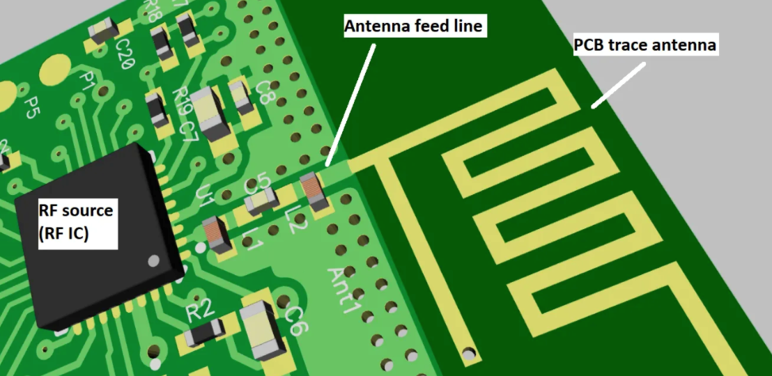
Figure 1: Example of a PCB/Trace Antenna design.
An embedded PCB antenna is a custom solution that is typically a metal trace printed onto the top layer of the PCB. Other types of PCB antenna designs require the trace to be laminated evenly across multiple layers on a board where vias are needed, to interconnect all the traces on each layer.
There are multiple key advantages with this antenna design approach. First, PCB antennas are the most cost-effective option to implement compared to all other internal antennas due to the fact that you are technically not purchasing a third-party component from a supplier. This is because the manufacturing cost of a PCB antenna is included in the PCB assembly process when a project is in the mass production phase. A second advantage of using a PCB antenna is that it is the lowest profile approach for internal antennas due to it being a part of the PCB’s surface. The only space a PCB antenna occupies is a copper-free surface where there is a sufficient amount of space for the antenna to be mounted (the antenna clearance area). However, keep in mind that because of this, the total area required is always much greater than the size of the metal trace itself which could be a potential waste of valuable PCB real estate.
Despite the affordable cost and low-profile benefits of PCB antennas, there are a couple of key drawbacks that can make them undesirable for certain projects. First, although they are a very simple design in principle, properly integrating them to achieve optimal performance for your specific PCB will require a considerable amount of RF design expertise–there is no “one fits all” approach for PCB antenna designs. Since the PCB antenna is part of the board itself and is entirely ground plane dependent, it makes it very susceptible to any subtle changes to the PCB size. Proximity to other components on the board can also cause undesirable effects to the antenna’s performance. Any slight variation in the PCB design could result in the antenna being detuned from its intended center frequency and cause overall signal reception issues. Furthermore, when comparing the RF performance of a PCB antenna to other internal antennas, their inherently simple design and extreme sensitivity make them the poorest performing option in terms of range. Additionally, since the antenna is integrated during the PCB manufacturing process, customers will have no flexibility in terms of optimizing the antenna’s performance. Consequently, it is common that multiple design iterations of the entire PCB will be required just to optimize the antenna, thus resulting in additional cost and development time for the customer
Chip Antennas
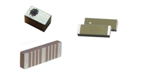
Figure 2: Ceramic Chip Antenna examples.
A chip antenna is made of ceramic and is the smallest, discrete type of internal antenna available. These antennas can be purchased as a separate component, which is one of their main advantages in comparison to that of a custom solution (such as a PCB antenna), as their performance optimization becomes easier and more flexible even after the chip antenna is integrated on the board. Chip antennas offer numerous features that contribute to their ease of optimization, including their impedance matching network and the option for additional ground clearance beneath the antenna to further adjust frequency tuning.
The antenna performance of a system will always require active measurements and tests in advance RF facilities, especially during the certification process. For PCB antennas, any adjustments will result in additional cost and time, as it will require the development of an entirely new PCB iteration. Comparatively, a chip antenna that is performing poorly would require a simple swap of the antenna or an adjustment to its impedance network components to resolve this issue.
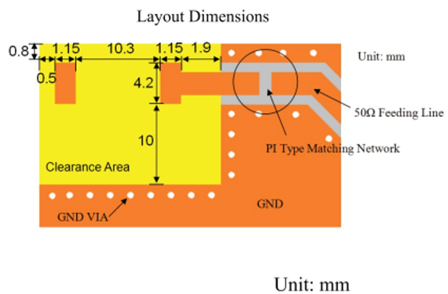
Figure 3: Example of Chip Antenna layout design (ground clearance area, impedance network, etc.).
Chip antennas are the most ideal solution for small IoT applications that have strict size requirements for the PCB. A typical trace antenna will not be suitable in this scenario because although they are very low profile, they would still require more space on the PCB to account for both the metal trace and the required ground clearance area beneath it. Conversely, chip antennas are better suited for small boards since they typically take up less PCB area, despite being thicker in size. Additionally, there are chip antennas that are designed to work on-ground, or over a copper layer (often called “over-metal”) of the PCB. These on-ground antennas require a more vertical design compared to their off-ground counterparts, fortunately without compromising radiation performance. This makes the chip antenna an even more viable solution for small form factor applications, as there will not be a need to increase PCB size to integrate them–thus saving on manufacturing costs. Chip antennas also boast superior performance when compared to a trace antenna, since they are less susceptible to detuning from other components or environmental factors that are within close proximity.
Although chip antennas have their benefits, they still come with a few disadvantages. One factor being their initial cost, since the customer will have to rely on a specific manufacturer to supply this component for mass production. Another prominent challenge that chip antennas present, is that despite them being easier to optimize, they are still very sensitive and are subject to similar design rules as trace antennas during integration. Finally, considerable RF design expertise would be required to achieve optimal system performance.
Examples of Chip Antennas available at Symmetry Electronics:
Patch Antennas
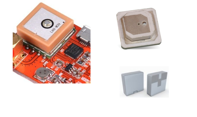
Figure 4: Patch Antenna examples.
A patch antenna, also known as a microstrip antenna, is essentially made up of two main layers: a ground plane at the bottom and a dielectric substrate on top. Upon the substrate layer lies a conductive patch including a specific geometry that serves as the radiating component that connects to the radio via a feedline. These antennas are popular due to their low profile, robust design, and stable performance for high volume applications. They are especially well-suited for very high frequency wireless protocols due to their physical dimensions that have a direct correlation with the wavelength. Additionally, the inherent design of patch antennas allow them to have a good amount of flexibility in terms of manufacturing and utilization.
There are multiple techniques that can be applied for feeding a patch antenna, including coaxial probe feeds, microstrip lines, aperture coupling, and proximity coupling. Each technique provides their own set of advantages in terms of ease of implementation, out-of-band spurious emissions, and bandwidth. Patch antennas are also diverse in terms of their polarization capabilities. Depending on their design, these antennas can be both linear and circular polarized (Dual Polarized). This is particularly useful for GNSS and satellite communication applications that typically rely on right-hand circular (RHCP) or left-hand circular (LHCP) polarizations for their antennas. The polarization of an antenna essentially describes the general direction of the electric field that is oscillating away from the source. Another unique feature of many patch antennas is that they can be integrated with ICs to effectively make them active antennas. The most common implementation is to have Low-Noise Amplifiers (LNA) embedded within these antennas to drastically improve signal reception. For example, this could be used to address weak satellite signals that are commonly found in GNSS applications. Additionally, this could be very useful for designers who typically have to design in the LNA as a separate external component on the antenna’s feedline–which effectively takes up more PCB space, often resulting in the need to increase the board size and ultimately increasing costs.
Although patch antennas have several advantages, they also have a few disadvantages. For example, when compared to other discrete surface mounted antennas (i.e. chip antennas), patch antennas would generally take up more PCB area/size. Additionally, if the patch antenna has an LNA integrated, you would have to take into account the additional power consumption of that active component.
Examples of Patch Antennas available at Symmetry Electronics:
- Taoglas Antennas: HP5010A, GPDF5012.A
- AVX Antennas: 1001039, 1002649
Flexible Printed Circuit (FPC) Antennas
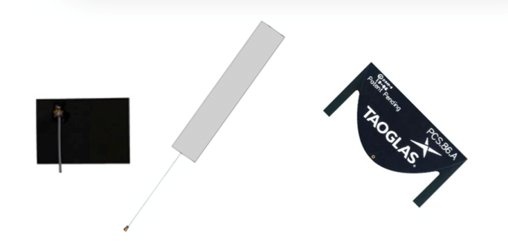
Figure 5: FPC Antenna examples.
Although FPC antennas are usually higher in price compared to other internal antenna options, being able to use them to bypass typical board design challenges could ultimately save time and engineering resources. The main design factors that have to be considered when using an FPC would be its cable length, as this would contribute to the FPC’s signal path loss and its proximity to the PCB ground plane when it is mounted within the housing.
Examples of FPC Antennas available at Symmetry Electronics:
- Taoglas Antennas: FXUB66.07.0150C, FXUB71.A.07.C.001
- AVX Antennas: 1002289, 1001932FT
Conclusion
With the increase in demand to make consumer electronics and many other embedded systems smaller, antenna suppliers are having to respond by developing a variety of diverse internal antenna options to support the unique requirements of new applications. Custom trace, ceramic chip, passive/active patch, and FPC antenna designs are all having to adapt to meet the demand of these shrinking devices. Due to this, it is very important that designers of these small-sized applications understand the specific advantages and drawbacks that each type of antenna has to offer. Factors during the design process like PCB area restrictions, product enclosure, minimum efficiency performance, cost, and access to RF expertise, are all crucial elements that must be considered prior to finalizing your internal antenna selection.