- Home
- Symmetry Blog
- The Case of the Noisy Source Clock Tree Part 2
From Silicon Labs: "Timing 101 #12: The Case of the Noisy Source Clock Tree Part 2"
About Symmetry Electronics
Established in 1998, Symmetry Electronics, a Division of Braemac, is a global distributor of electronic components and systems. Combining premier components and comprehensive value-added services with an expert in-house engineering team, Symmetry supports engineers in the design, development, and deployment of a broad range of connected technologies.
Exponential Technology Group Member
Acquired by Berkshire Hathaway company TTI, Inc. in 2017, Symmetry Electronics is a proud Exponential Technology Group (XTG) member. A collection of specialty semiconductor distributors and engineering design firms, XTG stands alongside industry leaders TTI Inc., Mouser Electronics, and Sager Electronics. Together, we provide a united global supply chain solution with the shared mission of simplifying engineering, offering affordable technologies, and assisting engineers in accelerating time to market. For more information about XTG, visit www.xponentialgroup.com.
Introduction
In this follow-up post, The Case of the Noisy Source Clock Tree Part 2, I will discuss in more detail exactly how to calculate the total jitter for a noisy source clock tree that includes a jitter attenuator. I will also provide a measurement and spreadsheet example.
Recap
In Part 1, I first discussed the low jitter source canonical clock tree, how to calculate the total jitter by Root Sum Square, and reviewed the terms jitter transfer, jitter generation, and additive jitter. I then moved on to the noisy source clock tree, the motivation for adding jitter attenuation, and introduced how to calculate its total jitter.
As I mentioned last time, following the clock signal from the source through the clock tree components to the sink or destination is best viewed as a system that processes phase noise. That is, if we know the phase noise characteristics of each clock tree component, we should be able to estimate the end clock phase noise and its phase jitter over a particular jitter bandwidth.
By best I mean that this approach is more universal and accurate. It can be applied to all types of clock trees, with or without noisy sources and jitter attenuators.
The Basic Idea
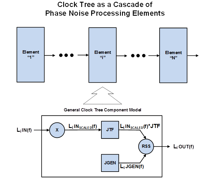
The general approach is illustrated below. Every clock tree can be regarded as a cascade of phase noise processing elements each of which, in the most general sense, can be modeled as the Root Sum Square or RSS of the Jitter Generation (JGEN) phase noise in contribution with the Jitter Transfer Function (JTF) applied to the scaled input clock phase noise.
Scaling is required so that the components contributing to the RSS are all at the same carrier frequency. The details will be made clearer in the example that follows.

The ith element above illustrates the general clock tree component model. All the contributions shown apply in the case of a jitter attenuator which also multiplies or divides the input clock. However, in practice, not all aspects of the general model apply, or are readily available, for every clock tree component:
- The independent clock source such as an XO at Element “1”, the root of the clock tree, has no input clock so the JTF branch is zeroed out. It can be modeled simply as JGEN, i.e. the source’s output clock phase noise.
- The typical clock generator has a wide bandwidth so the JTF contribution is negligible and it too is modeled simply as JGEN.
- The clock buffer has no PLL so JGEN is not applicable. Unfortunately, a JTF is usually not available. We typically have to rely on additive jitter specified over a particular bandwidth or do further characterization.
A Practical Measurement Example
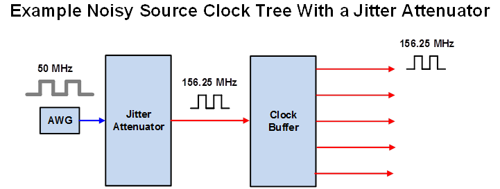
Consider the following simplified block diagram. I used an Arbitrary Waveform Generator or AWG as my noisy 50 MHz input clock source and followed it with an Si5345 evaluation board. The Si5345 does both jitter attenuation and clock multiplication as is the common practical case. I then followed the jitter attenuator (JA) with an Si53301 clock buffer evaluation board. The output clocks for both the jitter attenuator and clock buffer are 156.25 MHz.

No baluns or limiters were used. Just straightforward single-ended connections to and from test equipment and differential connections between the jitter attenuator and clock buffer. The unmeasured output clock polarity was terminated on the clock buffer EVB.
Calculating Phase Jitter
In the work that follows, we often want to calculate RMS phase jitter, i.e. integrated phase noise over a select frequency range, from a dataset of phase noise L(f) (dBc/Hz) versus offset frequency f (Hz). For the purpose of this exercise, we ignore spurs though they can certainly be included.
The general procedure is as follows.
- Convert SSB phase noise data L(f) from dBc/Hz to W/Hz.
- "Brickwall" filter the data over the selected jitter filter bandwidth. In this example, we take 12 kHz to 20 MHz. (Sloped filters can be used too but not in these particular spreadsheets.)
- Over the jitter filter bandwidth, take the average of the current and previous spot phase noise measurements (W/Hz) multiplied by the difference in offset frequencies (Hz).
- Sum all these jitter power contributions.
- Double to account for DSB or Double Sideband and then convert to UI or Unit Intervals.
- Finally, convert from UI to time domain units, typically fs.
As will be seen, the worksheets that use this technique calculate values very close to what the phase noise instrument reports.
Measurement Steps
I have attached a spreadsheet, PhaseJitterCalcsClockTreeWithoutSpurs.xlsx, that records the results and compares them to lab measurements in the form of Agilent E5052B screen caps. There are 9 total measurements steps listed below in worksheet order as follows with additional details. The convention on the calculations worksheets is that input data are in yellow colored cells.
1. 50 MHz AWG Meas Data - Measure the AWG’s 50 MHz phase noise. This is the clock phase noise that will be input to the jitter attenuator. This worksheet imports the CSV file containing the measured phase noise for an Arbitrary Waveform Generator (AWG) operating at nominal 0 dBm and 50 MHz.
2. 50 MHz AWG Calcs - Calculate the AWG’s 50 MHz phase jitter based on the measured phase noise data using the procedure described earlier.In this context, the term “phase jitter” always refers to the RMS quantity based on integrating phase noise over the 12 kHz – 20 MHz offset frequency range. The calculated result is 7917 fs or 7.7917 ps which is noisy indeed. This result is accurate to 0.1% compared to the figure reported by the Agilent E5052B screen cap.
3. 50 MHz Sig Gen Meas Data - Measure the signal generator’s 50 MHz phase noise. This worksheet imports the CSV file containing the measured phase noise for a signal generator also operating at nominal 0 dBm and 50 MHz.
Note: This is the clock phase noise that will be input to the jitter attenuator (JA) to estimate its Jitter Generation (JGEN) at the output frequency. It was presumed, based on previous experience, that the sig gen’s performance would be better than the AWG’s and so would be a good candidate for this role. However, this had to be confirmed.
4. 50 MHz Sig Gen Calcs - Calculate the sig gen’s 50 MHz phase jitter.The calculated result is 785 fs, accurate to 0.02% compared to the figure reported by the Agilent E5052B.
5. 50 MHz AWG vs Sig Gen Plots - Here I compare the AWG versus the signal generator phase noise, both operating at 50 MHz. Generally speaking the sig gen’s phase noise is close to, or better than, that of the AWG’s performance. The previous worksheets’ calculations showed that the signal generator was roughly an order of magnitude better than the AWG in terms of phase jitter. Given this confirmation, it is reasonable to select the sig gen to be the low noise source for the subsequently estimated JGEN.
Note: It may also be expedient to operate a jitter attenuator in Free Run mode and use its output clock phase noise as a stand-in for JGEN. It does not account for all noise sources but can often get within 5% for typical jitter bandwidths. However, it will not be as accurate at low offset frequencies.
6. JGEN 156.25 MHz Meas Data - This worksheet imports the CSV file containing the JA’s 156.25 MHz output clock measured phase noise where the low noise RF signal generator supplies the 50 MHz input clock. This data is used to the estimate the JA’s JGEN.
7. JGEN 156.25 MHz Calcs - Calculates the JA’s JGEN phase jitter. The calculated result is 83.5 fs, accurate to 0.03% compared to the figure reported by the Agilent E5052B.
8. Clock Tree Calcs - This is the clock tree calculations worksheet that puts everything together. Inspecting the columns going from left to right you can see the following operations:
- Scale the input clock phase noise with reference to the output clock carrier frequency.
- Apply jitter attenuation. Here we assume a low pass filter response with 40 dB /dec attenuation starting at the loop BW frequency 100 Hz. This is a simplified version, accurate well beyond the corner frequency. (The more accurate the JTF, the better the results.)
- Bring in the JGEN data from worksheet “7. JGEN 156.25 MHz Meas Calcs”.
- RSS the contributions from the JGEN phase noise plus the scaled jitter attenuated phase noise.
- Calculate the phase jitter for the JA’s output clock.
- Finally, calculate the phase jitter for the clock buffer’s output clock. There is no JTF for this buffer but there is a specified typical spec of 145 fs additive phase jitter, 12 kHz – 20 MHz.
Two different E5052B screen caps are copied on to this last calculations worksheet, one for the JA output clock, and one for the buffer output clock.
9. Clock Tree Plots - All of the relevant input, interim, and output curves for the jitter attenuator are plotted here.
Overall Results
So how did it go? It went reasonably well with a caveat at the end.
The JA output clock phase jitter was calculated to be 83.47 fs which was 0.9% lower than the measured 84.19 fs. The shape of the measured phase noise plot looks close to the expected plot except close in.
The buffer output clock phase noise was calculated to be 167.31 fs which was -5.2 % lower than measured, based on using the datasheet typical value for additive jitter, 12 kHz – 20 MHz. We don’t simply see +1 or +2 dB added everywhere to the JA output clock phase noise. Rather, the shape of the measured phase noise plot showed more phase noise at far offset frequencies, where the “floor” rose from about -162 to -152 dBc/Hz.
Bottom line: These results are good from a phase jitter point of view. However, it appears that a buffer JTF would be needed to better predict the end phase noise plot.
Conclusion
I hope you have enjoyed this Timing 101 article. This is the last post for 2018. Happy Holidays and Happy New Year to you all! I look forward to exploring more topics with you in 2019.
As always, if you have topic suggestions, or there are questions you would like answered, appropriate for this blog, please send them to kevin.smith@silabs.com with the words Timing 101 in the subject line. I will give them consideration and see if I can fit them in. Thanks for reading. Keep calm and clock on.
Cheers,
Kevin
Source: https://www.silabs.com/community/blog.entry.html/2018/12/21/timing_101_12_the-ikzY
