- Home
- Symmetry Blog
- From Silicon Labs - Timing 101: The Case of the PLL's VCO High Pass Transfer Function
From Silicon Labs - Timing 101: The Case of the PLL's VCO High Pass Transfer Function

About Symmetry Electronics
Established in 1998, Symmetry Electronics, a Division of Braemac, is a global distributor of electronic components and systems. Combining premier components and comprehensive value-added services with an expert in-house engineering team, Symmetry supports engineers in the design, development, and deployment of a broad range of connected technologies.
Exponential Technology Group Member
Acquired by Berkshire Hathaway company TTI, Inc. in 2017, Symmetry Electronics is a proud Exponential Technology Group (XTG) member. A collection of specialty semiconductor distributors and engineering design firms, XTG stands alongside industry leaders TTI Inc., Mouser Electronics, and Sager Electronics. Together, we provide a united global supply chain solution with the shared mission of simplifying engineering, offering affordable technologies, and assisting engineers in accelerating time to market. For more information about XTG, visit www.xponentialgroup.com.
Welcome to another edition of the Timing 101 blog from Silicon Labs' Kevin Smith.
We have been doing some internal training recently and a common question that comes up is how and why a Phase Locked Loop (PLL) treats phase noise differently depending on whether it comes from the input clock or the VCO (Voltage Controlled Oscillator). Most everyone understands that input clock phase noise is jitter attenuated, i.e. the PLL acts like a low pass filter to input phase noise. However, it is not as readily apparent why a PLL should act like a high pass filter to VCO phase noise. This is the Case of the PLL’s VCO High Pass Transfer Function and the subject of this month’s post.
First, I will review the basic feedback loop and its transfer function. Next, I will generalize the process for signals injected at different locations around the loop. I will then generate and compare the transfer functions for a PLL both from the input clock and the VCO perspective. Finally, I’ll wrap up by offering some intuition and discussing the application considerations.
Feedback Review
Consider the basic feedback diagram in the figure below where the variables and blocks are functions of the Laplace complex frequency variable ‘s’. The intermediate variable S representing error should be considered likewise. The forward gain is G(s) and the feedback gain H(s). I(s) and O(s) are the input and output signals respectively.
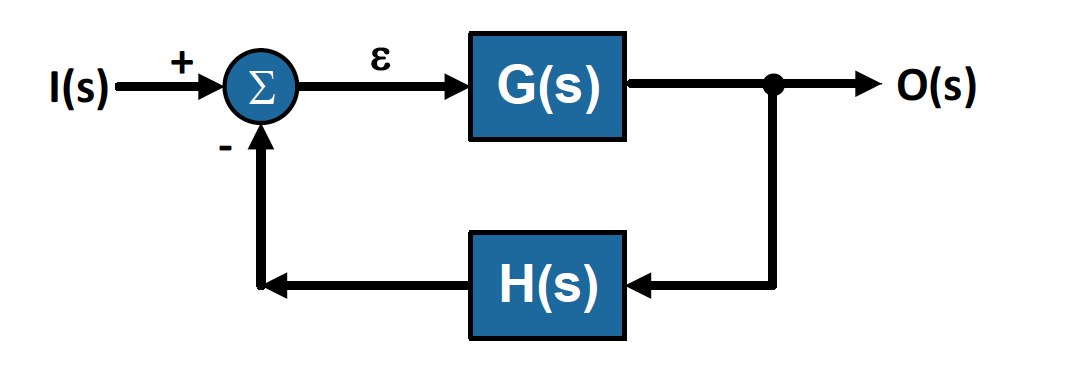
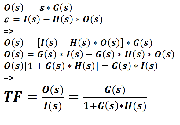
The closed loop transfer function TF for O(s)/I(s) is derived as follows.
Now what happens if we break up the forward path gain G(s) in to two separate blocks, G1(s) and G2(s) and inject a new signal X(s) as illustrated below? X(s) is additive as with noise.
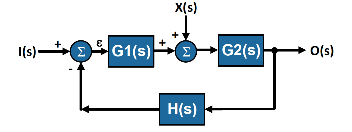
By linearity, the transfer function TF for O(s)/x(s) is derived as follows where I(s) is set to 0.
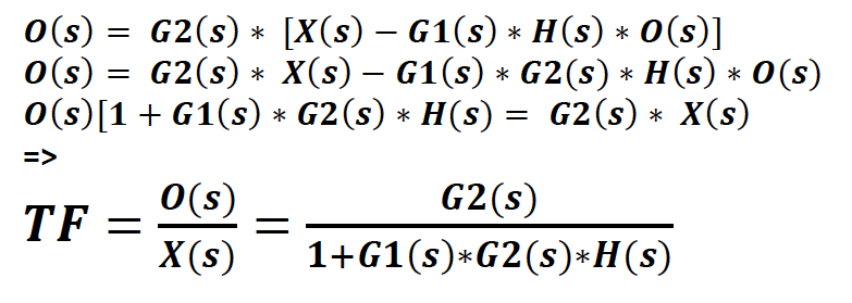
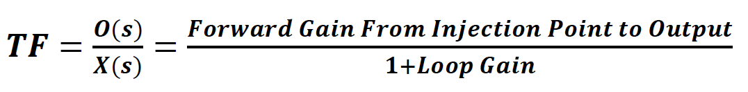
It turns out we can generalize for any X(s) injection point anywhere around the feedback loop as follows. The term “Loop Gain” refers to the multiplication of all the gain elements going around the closed loop. In this particular example, the Loop Gain = G1(s)*G2(s)*H(s).
We can now apply these developments to the basic PLL.
Input Clock Phase Noise Transfer Function
Consider the basic linear “small signal” PLL diagram below.
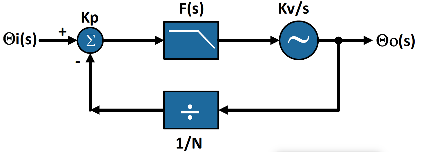
Going clockwise around the loop, the components in the diagram are as follows.
- Kp represents the gain of the phase detector, usually a PFD (Phase Frequency Detector).
- F(s) is the low pass filter as a function of complex frequency ‘s’.
- Kv is the gain of the VCO and the 1/s term represents the integration action of the VCO. That is, the Laplace transform of the integral of Kv*phase is Kv/s.
- 1/N is the gain of the feedback divider.
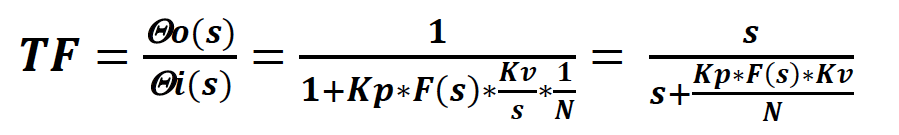
We can now generate the TF for Theta_o(s)/ Theta_i(s) almost by inspection by noting that the forward gain is KpF(s)Kv/s and the loop gain is [KpF(s)Kv/s]/N.
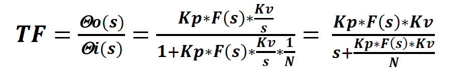
For reasons of stability F(s) is always a low pass filter so its value is either constant in value or rolls off with increasing frequency. In either case the overall closed loop behavior for the PLL is itself a low pass filter.
This PLL transfer function is covered in many textbooks and articles but a more detailed and recent discussion on this topic is contained in the article “Phase Locked Loop Noise Transfer Functions” by Peter Delos published in High Frequency Electronics, January, 2016.
VCO Phase Noise Transfer Function
Now consider the basic PLL diagram modified below to also inject VCO phase noise via variable Theta_v(s).
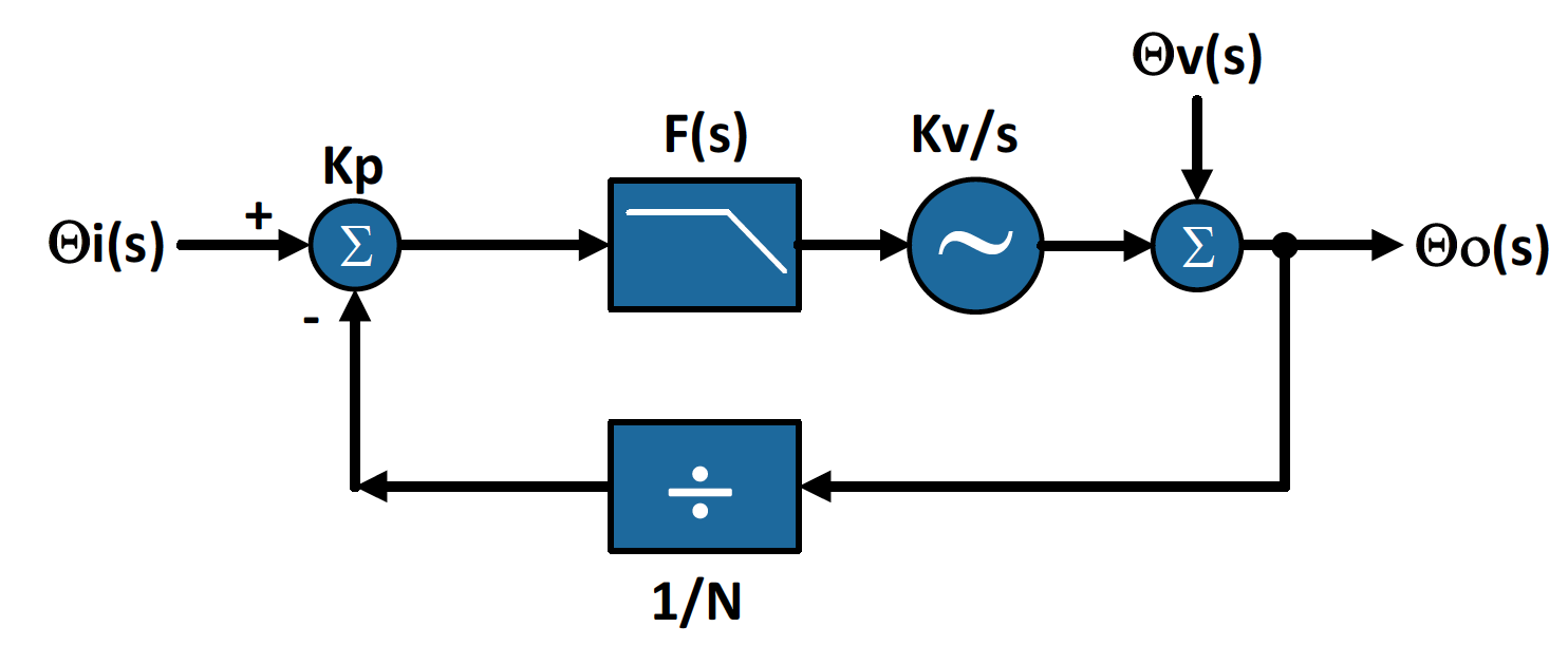
We can generate the TF for Theta_o(s)/ Theta_v(s) by noting that the forward gain from the VCO phase noise injection point is simply unity and the loop gain is [KpF(s)Kv/s]/N as before.
Again, F(s) is a low pass filter so it is either constant in value or rolls off. Unlike the transfer function for the input clock, the numerator here has a zero at the origin. In this case the overall closed loop behavior for the PLL is now a high pass filter.
Some Intuition
OK, I know some of you may be saying, I get the math but I don’t really, intuitively, understand why the PLL acts as a high pass filter to VCO phase noise. Let me offer some food for thought that may provide some intuition.
Consider the expected difference in behavior for a phase step at Theta_i versus Theta_v:
- We know that a phase step at Theta_i is not immediately output at Theta_o. Rather, it will take some time, depending on the loop bandwidth, for the PLL to respond and properly step the output phase to track the change in the input clock’s phase. This is analogous to a voltage step applied to a low pass filter.
- By contrast, a phase step at the output due to Theta_v must be immediately output at Theta_o. There is nothing to prevent this. The loop then has to put things right in order to correctly track the input clock again. Depending on the loop bandwidth, it will take time for the output clock to lose the excess phase. This behavior is analogous to a voltage step applied to a high pass filter.
Application Considerations
The 2 dominant sources of phase noise in a PLL are typically the input clock and the VCO. As we have seen, the PLL treats each source's noise differently, i.e. as a low pass and a high pass filter respectively.
The application consequences are as follows:
1. If an input clock has relatively low phase noise versus the VCO, one typically uses a relatively wide bandwidth (BW) PLL in order to attenuate the VCO's phase noise. In this context, a wide bandwidth typically means something on the order of 100s of kHz to MHz. This is how clock generators or clock multipliers are designed. (Note that BW cannot be arbitrarily large for reasons related to stability and the need to suppress phase detector spurs.)
2. On the other hand, if an input clock has relatively high phase noise versus the VCO, one typically uses a relatively narrow bandwidth PLL in order to attenuate the input clock's phase noise. In this context, a narrow bandwidth means something on the order of kHz or less, usually much less. This is how jitter attenuators are designed.
Understanding this tradeoff and the ability to adjust the bandwidth "knob" is a key to troubleshooting PLLs and optimizing their application.
Conclusion
This month I’ve reviewed how a PLL's VCO phase noise transfer function arises and its unique high pass behavior. I’ve also offered some intuition and discussed the application considerations.
I hope you have enjoyed this Timing 101 article. It’s the last post for 2017. Happy Holidays and
Happy New Year to all of you!
As always, if you have topic suggestions, or there are questions you would like answered, appropriate for this blog, please send them to kevin.smith@silabs.com with the words Timing 101 in the subject line. I will give them consideration and see if I can fit them in. Thanks for reading.
Keep calm and clock on.
Cheers,
Kevin
Source: https://www.silabs.com/community/blog.entry.html/2017/12/19/timing_101_the_case-xeSO


About Symmetry Electronics
Established in 1998, Symmetry Electronics, a Division of Braemac, is a global distributor of electronic components and systems. Combining premier components and comprehensive value-added services with an expert in-house engineering team, Symmetry supports engineers in the design, development, and deployment of a broad range of connected technologies.
Exponential Technology Group Member
Acquired by Berkshire Hathaway company TTI, Inc. in 2017, Symmetry Electronics is a proud Exponential Technology Group (XTG) member. A collection of specialty semiconductor distributors and engineering design firms, XTG stands alongside industry leaders TTI Inc., Mouser Electronics, and Sager Electronics. Together, we provide a united global supply chain solution with the shared mission of simplifying engineering, offering affordable technologies, and assisting engineers in accelerating time to market. For more information about XTG, visit www.xponentialgroup.com.