- Home
- Symmetry Blog
- From Micronas: "ICsense files new patent on zero-leakage high-voltage analog switches"
From Micronas: "ICsense files new patent on zero-leakage high-voltage analog switches"
About Symmetry Electronics
Established in 1998, Symmetry Electronics, a Division of Braemac, is a global distributor of electronic components and systems. Combining premier components and comprehensive value-added services with an expert in-house engineering team, Symmetry supports engineers in the design, development, and deployment of a broad range of connected technologies.
Exponential Technology Group Member
Acquired by Berkshire Hathaway company TTI, Inc. in 2017, Symmetry Electronics is a proud Exponential Technology Group (XTG) member. A collection of specialty semiconductor distributors and engineering design firms, XTG stands alongside industry leaders TTI Inc., Mouser Electronics, and Sager Electronics. Together, we provide a united global supply chain solution with the shared mission of simplifying engineering, offering affordable technologies, and assisting engineers in accelerating time to market. For more information about XTG, visit www.xponentialgroup.com.
ICsense, a TDK group company, is a leading supplier of analog, mixed-signal and high-voltage ASICs (Application Specific ICs). The company has filed another patent to strengthen its portfolio in innovative analog circuits. The invention allows to implement analog, floating high-voltage switches that don’t load its connected lines. Contrary to existing solutions using large resistances and thereby large time constants, this invention provides a solution with no leakage current and with a small time constant. It is particularly of interest for low-ohmic (low RDSon) switch matrix architectures for the medical, automotive, industrial and consumer markets.

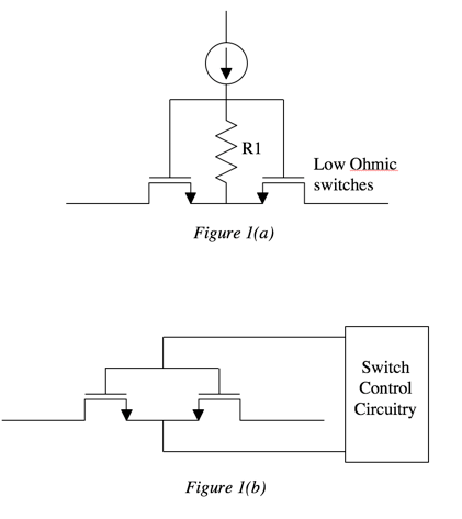
High current switch matrix topologies require the use of low-ohmic (D)MOS switches. The desire to have fast switching times (small time constant, small R1) and low leakage (large R1) can not be accomplished with a traditional architecture due to the conflicting requirement on R1 (as shown in Fig 1a). “We have designed a novel circuit to eliminate this conflicting requirement and are able to reach fast switching while having virtually zero-leakage. Moreover, in this classical floating pass-switch design the connected lines are loaded when the switch is enabled/disabled. This results in unwanted and inaccurate readings in applications such as high-impedant, high-voltage multiplexers and high-accuracy, high-voltage readouts like piezo-electrical transceivers” says Tim Piessens, CTO of ICsense.
“We will use this patent to offer ASICs to our customers with increased accuracy and at the same time fast switching and zero-leakage. Our newest patent applies to single MOS switches and to back-to-back topologies that allow full-range isolation,” says Tim. The design is particularly interesting for applications with low RDSon requirements (<5 Ohm) and heavy constraints on point loading. Additionally, high-voltage switch architectures benefit from the patent because it can cope with negative voltages and polarity changes.
In the past, ICsense has patented other inventions to stay ahead of competition. To produce more cost effective wafers, the company patented a circuit (patent nr BE1024217(A1)) which intelligently regulates stacked transistors to provide higher voltage swing (both drive and sense) in plain CMOS processes. The principle uses complex control techniques to guard the SOA (Safe Operating Area). With this invention it is possible to elevate the operational voltage of a plain low-cost CMOS process1 by a factor of x4. Since 2010, this patent is exploited in ICs which are in mass production by companies such as NVidia.
1In a standard 0.18um process, ICsense is able to provide 10V operational swing.
Bert Serneels, Eldert Geukens, Bram De Muer and Tim Piessens, "A 1.5W, 10V Output Class D Amplifier Using a Boosted Supply from a Single 3.3V Input in standard 1.8V / 3.3V 0.18µm CMOS", ISSCC Digest of Technical Papers, Feb 2012.


