- Home
- Symmetry Blog
- From Electronic Products: System integration considerations for heart rate sensing designs
From Electronic Products: System integration considerations for heart rate sensing designs

About Morrie Altmejd
Designing an optical heart rate monitoring (HRM) system, also known as photoplethysmography (PPG), is a complex and multidisciplinary undertaking. Design factors include human ergonomics, signal processing and filtering, optical and mechanical design, low-noise signal receiving circuits, and low-noise current pulse creation.
Wearable manufacturers are increasingly adding HRM capabilities to their health and fitness products, which is helping to drive down the cost of sensors used in HRM applications. Many HRM sensors now combine discrete components such as photodetectors and LEDs into highly integrated modules. These modules enable a simpler implementation that reduces the cost and complexity of adding HRM to wearable products.
Wearable form factors are steadily changing as well. While chest straps have effectively served the health and fitness market for years, HRM is now migrating to wrist-based wearables. Advances in optical sensing technology and high-performance, low-power processors have enabled the wrist-based form factor to be viable for many designs. The HRM algorithms have also reached a level of sophistication to be acceptable in wrist form factors.
Other new wearable sensing form factors and locations are emerging — such as headbands, sport and fitness clothing, and earbuds. However, the majority of wearable biometric sensing will be done on the wrist.
HRM design fundamentals
No two HRM applications are alike. System developers must consider many design tradeoffs: end-user comfort, sensing accuracy, system cost, power consumption, sunlight rejection, how to deal with many skin types, motion rejection, development time, and physical size. These design considerations impact system integration choices: whether to use highly integrated modules or architectures incorporating more discrete components.
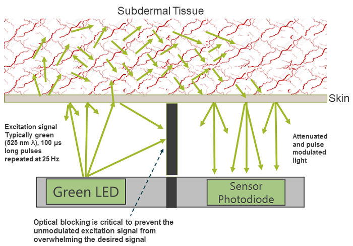 Fig. 1: Principles of operation for optical heart rate monitoring.
Fig. 1 shows the fundamentals of measuring heart rate signals, which depend on the heart rate pressure wave being optically extracted from tissue. It displays the travel path of the light entering the skin. The expansion and contraction of the capillaries — caused by the heart rate pressure wave — modulate the light signal injected into the tissue by the green LEDs.
The received signal is greatly attenuated by the travel through the skin and is picked up by a photodiode and sent to the electronic subsystem for processing. The amplitude modulation due to the pulse is detected, analyzed, and displayed.
A fundamental approach to HRM system design uses a custom-programmed, off-the-shelf MCU that controls the pulsing of external LED drivers and simultaneously reads the current output of a discrete photodiode. Note that the current output of the photodiode must be converted to voltage to drive analog-to-digital (A/D) blocks. The schematic in Fig. 2 shows the outline of such a system.
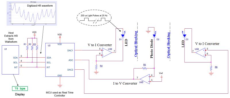 Fig. 2: The basic electronics required to capture optical heart rate.
Here, it’s worth noting that the I-to-V converter creates a voltage equal to VREF at 0 photodiode current, and the voltage decreases with increasing current.
HRM building blocks
The current pulses generally used in heart rate systems are between 2 mA and 300 mA, depending on the color of the subject’s skin and the intensity of sunlight with which the desired signal needs to compete. The infrared (IR) radiation in sunlight passes through skin tissue with little attenuation, unlike the desired green LED light, and can swamp the desired signal unless the green light is very strong or unless an expensive IR blocking filter is added.
Generally speaking, the intensity of the green LED light, where it enters the skin, is between 0.1 and three times the intensity of sunlight. Due to heavy attenuation by the tissue, the signal that arrives at the photodiode is quite weak and generates just enough current to allow for a reasonable signal-to-noise ratio (SNR) — 70 to 100 dB — due to shot noise even in the presence of perfect, noise-free op-amps and A/D converters.
The shot noise is due to the finite number of electrons received for every reading that occurs at 25 Hz. The photodiode sizes used in the design are between 0.1 mm2 and 7 mm2. However, above 1 mm, there are diminishing returns due to the effect of sunlight.
The difficult and costly function blocks to implement in an optical heart rate system design, as shown in Fig. 2, are the fast, high-current V-to-I converters that drive the LED, a current-to-voltage converter for the photodiode, and a reliable algorithm in the MCU that sequences the pulses under host control. A low-noise LED driver — featuring 300 mA and 75–100 dB SNR — that can be set to very low currents down to 2 mA while still creating very narrow light pulses down to 10 µs is an expensive block to achieve with discrete op-amps.
The narrow pulses of light down to 10 µs, shown in Fig. 2, allow the system to tolerate motion and sunlight. Typically, two light measurements are made for each 25-Hz sample. One measurement is taken with LEDs turned off and one with LEDs turned on. The calculated difference removes the effect of ambient light and gives the desired raw optical signal measurement that is insensitive to the flickering background light.
The short duration of the optical pulses both allows and requires a relatively strong light pulse. It is essential to stay brighter than the sunlight signal, which may be present and not allow the PPG signal carrier to be dwarfed by the sunlight signal.
If the sunlight signal is larger than the PPG carrier, then although it may be removed by subtraction, the signal can be so large that external modulation such as swinging an arm in and out of shadow can create difficult-to-remove artifacts. As a result, systems that use low-current LED drivers and large photodiodes can suffer severely from motion artifacts in bright-light situations.
Discrete vs. integrated design
Much of the desired HRM sensing functionality is available pre-designed and integrated into a single device. Packing most of this functionality into one piece of silicon results in a relatively small 3 x 3-mm package that can even integrate the photodiode itself.
Fig. 3 shows an example of a schematic with an optical sensor. This HRM design is relatively easy to implement. You just need to focus on the optical portion of the design, which includes optical blocking between the parts on the board and coupling the system to the skin.
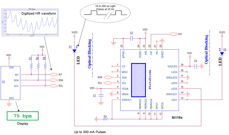 Fig. 3: An integrated heart rate sensor requires only external LEDs.
While the approach shown in Fig. 3 results in a high-performance HRM solution, it’s not as small or power-efficient as some designers would like. To achieve an even smaller solution, the LED die and the control silicon must be integrated into a single package that incorporates all essential functions, including the optical blocking and the lenses that improve the LED output. Fig. 4 illustrates this more integrated approach, based on a Silicon Labs Si117x optical sensor.
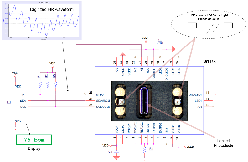 Fig. 4: A highly integrated HRM sensor module incorporating all essential components.
No external LEDs are required for this HRM design. The LEDs and photodiode are all internal to the module, which can be installed right below the optical ports at the back of a wearable product such as a smartwatch. This approach enables a shorter distance between the LEDs and photodiode than is possible with a discrete design. The reduced distance allows operation at extremely low power due to lower optical losses traversing the skin.
Integrating the LEDs also addresses the issue of light leakage between the LEDs and photodiode so that the designer doesn’t have to add optical blocking to the PCB. The alternative to this approach is to handle the blocking with plastic or foam inserts and special copper layers on the PCB.
There is one more part of an HRM design that developers don’t necessarily need to create: an HRM algorithm. This software block residing on the host processor is quite complex due to the signal corruption that occurs during exercise and motion in general. End-user motion often creates its own signal that spoofs the actual heart rate signal and is sometimes falsely recognized as the heart rate beat.
If a wearable developer or manufacturer doesn’t have the resources to develop the algorithm, third-party vendors provide this software on a licensed basis. It is up to the designer to decide how much integration is right for the HRM application. The developer can simplify the design process and speed time-to-market by opting for a highly integrated module-based approach using a licensed algorithm.
Developers with in-depth optical sensing expertise, time, and resources may opt to use separate components — sensors, photodiodes, lenses, etc. — and do their own system integration and even create their own HRM algorithm.
Learn more about Silicon Labs