- Home
- Symmetry Blog
- 7 Tips on Best Antenna Placement for Surface-Mounted Chip Antennas | Symmetry Blog
7 Tips on Best Antenna Placement for Surface-Mounted Chip Antennas | Symmetry Blog

About Augustine Nguyen
For any antenna, proper placement is fundamental to optimal performance. The best antenna on the market won’t do your application any good if it is not used in the right way. This is especially the case for surface-mounted chip antennas, which demand specific criteria for optimal performance.
In order to help engineers make the most of their antennas, I have compiled 7 important tips for ideal antenna placement.
But first, when would you use a chip antenna?
Typically, surface-mounted chip antennas are best used when the PCB of the application is extremely small. When this is the case, chip antennas are your best bet for adding wireless capabilities to your design. They offer a small form factor that take up minimal space on the PCB and can still offer great performance.
Chip antennas are typically offered off-the-shelf, so you can find a variety of them to fit your PCB design.
So now you might be wondering, “Where do I place my antenna for optimal performance?”
Here are 7 tips on best antenna placement:
1. Follow the reference board to match datasheet performance
While the performance shown on the datasheet may look great, just putting the antenna anywhere on the PCB won’t get you the same results if you do not take placement and board size into consideration. One of the best ways to get datasheet performance out of the antenna is by following the reference board design as closely as possible. The reference board provides an easy template to follow without spending a lot of time and effort on the engineer’s part. Following the reference board helps highlight and avoid the most important factors when using chip antennas, such as PCB size and ground size sensitivity.
Of course, it’s not always possible to follow the reference board exactly. In such cases, be sure to follow the other principles of best antenna placement below.
2. Always place the antenna at the edge of the PCB with sufficient clearance from the rest of the circuit
The antenna should be placed at the edge of the PCB, away from the rest of the circuit. Due to the sensitivity of antennas, providing the antenna with sufficient clearances reduces the possibility of electromagnetic interference from other high-frequency components, like power ICs, clock generators, and other signal busses.
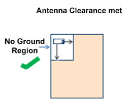
3. Don’t place the antenna directly above any ground layers on the PCB
Antennas should not be placed above any ground layers on the PCB. The metal layer beneath would affect how signals are propagating, disrupting the antenna’s functionality.
You can often find the recommended antenna clearances proposed and evaluated in the antenna’s data sheet.
4. Make sure the antenna is not covered by a metallic enclosure
Do not place the antenna in a location where it is completely covered by a metallic enclosure. This would cause significant shielding to the antenna. If the product does have a metallic casing or a shield, the casing must not cover the antenna. Note that no metal is allowed in the antenna near-field.
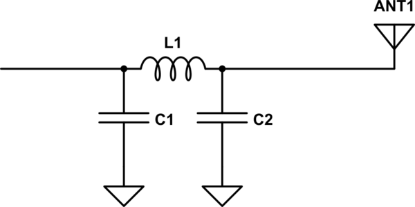
5. Leave extra space for the antenna’s matching network
When planning the placement of the antenna, take into account the extra space needed for the antenna’s matching network. A lot of parameters in the antenna’s proximity (enclosure, ground variation, substrate differences, and other components) can vary its impedance. Implementing a PI or T network in your design will give you the freedom to further tune the antenna if needed (see below image).
When first adding a PI or T network, compose a series of three components with 0 ohms resistors to make it more flexible in the future if further tuning is needed. Refer to the diagrams below.
 PI-NETWORK
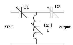 T-NETWORK
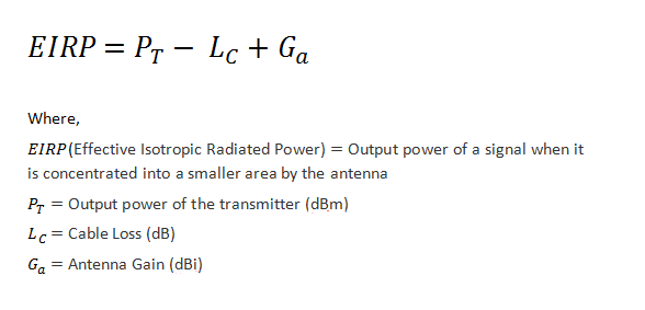
6. Place the antenna, impedance matching network, and radio output as close to each other
Putting these three into proximity to each other helps to ensure a low signal loss from chip to antenna.
The key to implementing this is achieving EIRP (effective isotropic radiated power), taking into account the signal loss from the chip output to antenna feed
7. Plan ahead with the placement of the antenna early during the design process to achieve optimal spacing
Nothing is more important to the design cycle than proper planning. Understanding how the antenna needs to be placed in the early stages of design will save the engineers a lot of time and resources in the future, but not all engineering teams have a specialist who is knowledgeable enough with antenna parts. Luckily, Symmetry offers free applications support for all kinds of electronics, including wireless solutions and antennas. Contact our team of applications engineers today to get free support on your next design.
Recommended antenna products
One of our trusted suppliers for antennas is Ethertronics, whose breakthrough Active Steering technology combines their patented Isolated Magnetic Dipole™ (IMD) antenna technology with their active antenna systems approach. Ethertronics provides users with the ability to generate multiple radiation patterns from a single antenna structure. A patent-pending algorithm then samples and switches between the radiation patterns to select the best one in response to the specific environment. The resulting Active Steering technology dynamically responds to changing RF conditions – fast enough to minimize multipath fading and, in turn, increase both download speeds and connectivity.
For ISM/BT/GPS:
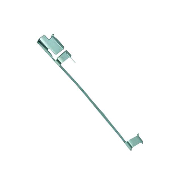
Ethertronics’ 1002427 stamp metal SMT antenna delivers the device designers’ key needs for higher functionality and performance in smaller/thinner designs. This innovative antenna provides compelling advantages for all ISM, Bluetooth and GPS enabled devices.
For LTE:
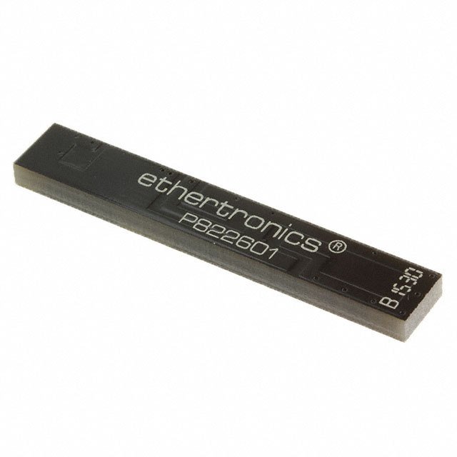
Ethertronics’ Universal Broadband Embedded LTE/LPWA antenna utilizes Isolated Magnetic Dipole™ (IMD) technology which address the challenges facing today’s product designers. IMD’s high performance and isolation characteristics offer better connectivity and minimal interference.
For WLAN/BT/Zigbee:
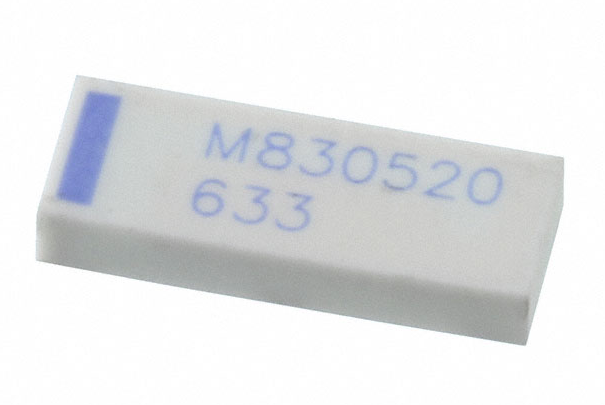
Ethertronics’ series of Ceramic Isolated Magnetic Dipole™ (IMD) antennas deliver on the key needs of device designers for higher functionality and performance in smaller/thinner designs. These innovative antennas provide compelling advantages for a full WIFI dual band enabled handheld devices, media players and other mobile devices.